A transistor adapter circuit without need for external power supply converts Morse sound output to switch signals for the CW-keyer input of modern ham radio transceivers. In a simple variation, Morse sound signals directly drive the base of an all-purpose NPN transistor. Alternatively, a more robust design features a transformer and rectifier stage for improved switching signal accuracy and galvanic isolation.
The design idea of the two adapter circuits is to use the voltage on the transceiver’s keyer jack as a power supply.
Simple CW-Keyer Adapter

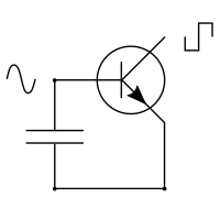
The most basic solution coming to mind has the sound card signal directly on the base of the switching NPN transistor. On the left hand side of Figure 1, the sound card of a laptop that generates the Morse code audio connects to the circuit. To the right it’s the keyer input of the transceiver.
In order to drive the base, Morse audio generators need to deliver signal levels above base voltage threshold. This should be no problem with computer sound cards. For instance, my laptop produces sound signals above 3.4 V peak to peak. As a switching transistor, BC 337 can be swapped with a wide variety of general-purpose NPN types.
On the Yaesu FT 991, Yaesu FT-DX 10, and Icom 7300 ham radio transceivers I tested, the keyer inputs correspond to voltage sources of +3 to +5 V with internal resistances of several kilo ohms. Consequently, the adapter has no need for an additional power supply and any NPN transistor can handle the low switching currents.
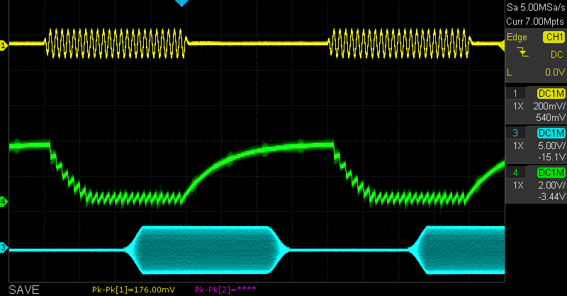
Figure 2 shows top yellow the Morse sound signal (in vertical scale 1:10), the keyer input / collector voltage green in the middle, and the transmitter output light blue on the bottom. Horizontally, one grid square is 10 milliseconds. In the adapter’s input path, the 4.7 kΩ and 4.7 nF constitute a low pass. On the output side the purpose of the 1 μF electrolyte capacitor is to cover the gaps between peaks of the sound signal.
Downsides of the Simple Adapter Design
Because the transistor only conducts in its emitter-collector path when the base voltage crosses a threshold of roughly 0.6 V, a saw-tooth pattern is superimposed on the active sections of the green switch signal. At a side tone frequency of 600 Hz, gaps have lengths of about 1.5 ms. Therefore, the capacity on the collector side is not an easy choice. It needs to be big enough to sufficiently suppress the saw-tooth. But not be too big because otherwise the keyer voltage does not recover quickly enough during Morse code spaces.
The problems in finding a good value for the collector side capacitor is a fundamental weakness of the simple adapter. To make matters worse, the internal resistance of the keyer voltage source will differ between transceiver brands and models. So the 1 μF which I picked for my FT-DX 10 and speeds of up to 30 wpm may not be applicable to other use cases.
However, one could simply increase the frequency of the Morse sound signal up to 8 kHz. This would shorten the gaps and allow for much lower capacities to still suppress the saw-tooth.
Robust CW-Keyer Adapter Design with Transformer and Rectifier
The more robust version of the adapter avoids the problems of finding a good value for the collector capacitor. Because of a 1:10 to 1:20 transformer, the audio voltage becomes high enough for a rectifier bridge. Past the rectifier stage the audio frequency doubles and therefore the gaps in the base current of the switching transistor shorten. Thus, it is easier to balance short keyer voltage recovery times against suppressing the saw-tooth signal. What’s more, the load capacitor covering the gaps has moved from collector to the base side of the transistor. As a consequence, the resistance discharging the load capacitor no longer depends on the transceiver model. So, the values of 33 nF and 100 kΩ should suit most everyone.

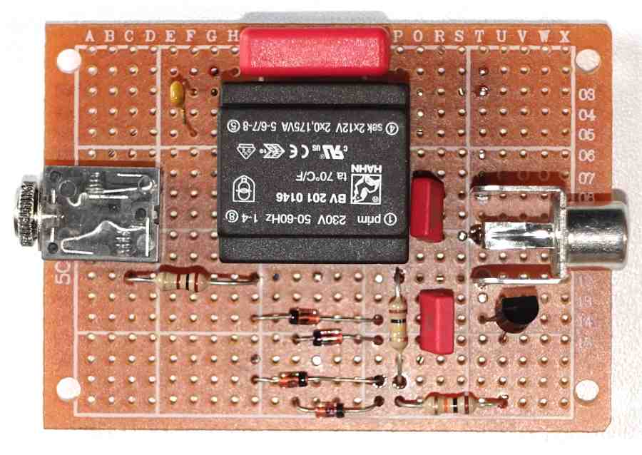
Since audio frequency transformers are getting rare, I just used a small sized power transformer. Translation ratios between 1:10 and 1:20, like 12V:230V, do the trick. Switching transistor and rectifier diodes can again be swapped for other general purpose types. If galvanic insulation is not important, one could replace the 470 nF capacitor with a wire bridge. Otherwise, a relatively large capacity needs to prevent interfering signals between the ground connectors from triggering the rectifier stage.
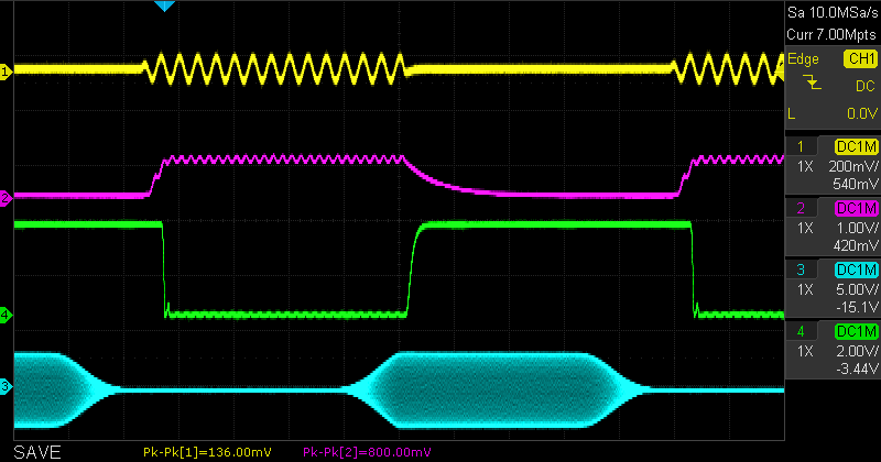
Signals for the more robust adapter converting Morse sound to CW-keyer input are shown in Figure 5. As expected, ripples on the purple driver voltage have double the sound frequency because of the rectifier.
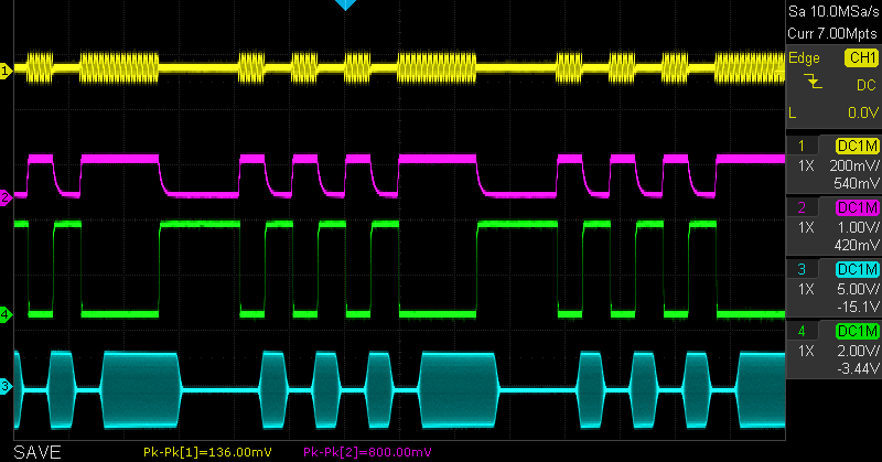
Overall, the robust adapter produces a clean switch signal with balanced dot and space ratio.
Conclusion
Electronic adapter circuits to turn computer generated Morse code audio into transceiver suitable switch signals are easy to implement. Without need for external power supply, as well as optional galvanic input and output separation, the design minimizes the risk of short-circuit faults, which is great for portable operation. And for self-written Morse code software, audio streams are a good choice to achieve millisecond precision signal timing.